CIRCUIT DESCRIPTION
The G4CLF Transceiver is the heart of a simple, but high performance, SSB transceiver system developed in the Applications Laboratories of Plessey Semiconductors Ltd in the late 1970s and published in 1980. It uses the Plessey Semiconductors' SL1600 family of integrated circuits for radio systems, which was made obsolete in the early 1990s. These circuits are virtually unobtainable today and this transceiver should not be attempted unless you have more than sufficient ICs to build it. This web-page is maintained for the benefit of people who already have a G4CLF transceiver, and
not to encourage anyone to build one.
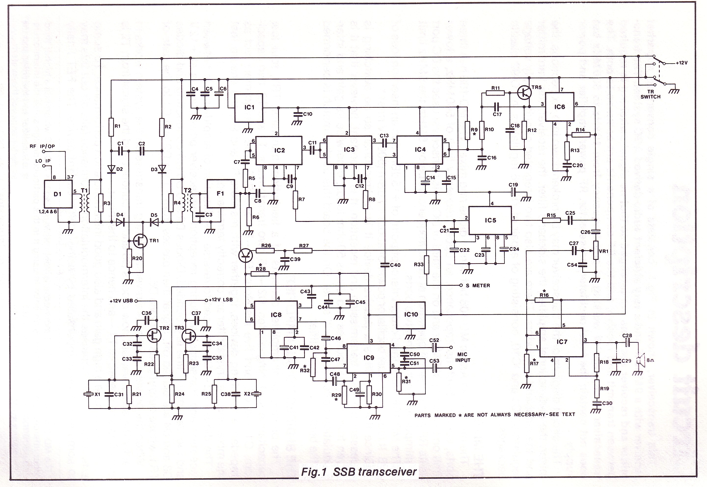
The transceiver, shown in Fig.1, consists of a single conversion superhet receiver with a 9MHz IF and a very efficient audio-derived AGC system. The transmitter and receiver sections are arranged so that no signal switching is required between transmit and receive, and the RF components are common to both. The transceiver board is capable of working at any frequency from 10 kHz to 500 MHz but does not contain the local oscillator, preselector, RF power amplifier and power supply.
The circuit diagram of the transceiver may be broken down into six sections: the mixer, the bi-directional amplifier, the sideband filter, the receiver, the transmitter, and the sideband oscillators. There are also two integrated circuit supply voltage regulators, IC1 and IC10, consisting of a pair of 78L06 regulators.
 THE MIXER
The mixer is an Anzac MD-108 hot carrier diode ring mixer. The MD-108 has three ports, each of 50 ohms impedance, an upper frequency limit of 500 MHz, a lower limit on two ports of 5 MHz and on the third of DC. This transceiver uses the DC port as its RF port to permit operation at radio frequencies below 5MHz; the 5MHz limit is unimportant on the other two ports.
The MD-108 has a third-order intercept point of +15dBm and an insertion loss of 7dB. It requires a local oscillator power of about +7dBm (500mV rms)
1.
Since the MD-108 is a passive device it is bi-directional, so no switching is necessary between transmission and reception. It is important, however that it is driven from 50 ohm sources and drives 50 ohm loads, otherwise its gain and intermodulation performance will suffer. On the board this 50 ohm match is performed by the bi-directional amplifier.
THE BI-DIRECTIONAL AMPLIFIER
The bi-directional amplifier consists of a field-effect transistor, TR1, four low capacitance switching diodes, D2-D5, two transformers, T1 and T2, two capacitors, C1 and C2, and five resistors, R1-R4 and R20. The transformers act as impedance matching devices, together with resistors R3 and R4, and ensure that the mixer and the crystal filter are correctly terminated.
The diodes D2--D5 are used to reverse the direction of amplifier gain between reception and transmission. During reception the receiver power line is at + 12V and the transmitter line is grounded. Diodes D2 and D5 are conducting and diodes D3 and D4 are biased off. Signal then passes from T1 via D2 and C1 to the gate of TR1, whose output goes to T2 via D5.
When the power supplies are reversed during transmission the system works in exactly the same way but now diodes D3 and D4 conduct and the signal from T2 is amplified and passed to T1 - and hence to the mixer.
TR1 must have a high gain and also good intermodulation performance. To some extent as the gain increases the intermodulation performance falls off but this effect may be minimised by using a high current device The FET finally chosen was a Siliconix J310. This is a VHF junction FET in a TO-92 package which has a standing current at zero gate bias of between 20 and 60 mA.
THE FILTER
This design uses an XF9-B or a QC1246AX crystal filter. These filters (manufactured by KVG and Salford respectively) are 8 pole 2.4 kHz filters with a centre frequency of 9 MHz. They require terminations of 500 ohms in parallel with 25 pF which is provided by T2, R4 and C3 on the mixer side of the filter and R6 and C8 on the other side.
Many other filters might be used in this transceiver but there are a number of points to be considered. If a 4 pole or a 6 pole filter is used the stop band suppression is reduced from over 90 dB to as little as 50 dB This can degrade adjacent channel performance and lead to intermodulation problems in the IF from very strong local signals but these are compromises which may be acceptable. Another problem can arise from the use of cheaper 4 pole or 6 pole filters which is not acceptable - they can allow blocking due to local oscillator leakage. The MD-108 has local oscillator attenuation of about 40 dB which means that there may be 5 mV rms of local oscillator signal present at its output and therefore some 25 mV rms at the input to the filter. If the filter attenuation is 90 dB this signal is reduced to less than 0.8 microvolts which is unimportant. If the attenuation is only 50 dB then the IF strip sees 80 microvolts of local oscillator leakage. If the transceiver is being used at VHF this is unimportant since the SL1612s in the IF strip have no gain at VHF but in an HF transceiver this 80 microvolts may be sufficient to block the IF strip, particularly if no AGC is present. The conclusion is obvious: at VHF lower performance filters may be used - at HF they may not.
Other intermediate frequencies than the 9 MHz used here are perfectly acceptable. The system will work unchanged at 5.3 MHz and 10.7 MHz but IFs of over 15 MHz or under 5 MHz cannot be used. Above 15 MHz the gain of the IF amplifier starts to drop and below 5 MHz the MD-108 mixer loses gain. There is no way of extending the upper frequency limit but the lower one may be reduced by either of two methods.
One method is to use the DC port of the MD-108 as the IF port. This allows the use of any IF down to 100 kHz but prevents the use of RF or local oscillator frequencies below 5 MHz which may or may not be a disadvantage. It will also be necessary to modify the printed circuit board layout.
The other method for reducing the lower frequency limit is to replace the MD-108 with an MD-109. This is a lower frequency version of the MD-108 which is rather more expensive but has a frequency response from 200 kHz to 200 MHz. While it is possible to use IFs down to 200 kHz using an MD-109, it is not possible to work with RFs above 200 MHz. This is unlikely to be a problem since the use of IFs below 5 MHz with RFs above 200 MHz is likely to lead to image problems and thus will tend to be avoided anyway.
If the transmitter performance is not to be degraded the bandwidth of the filter must not exceed 2.7 kHz and the shape factor should be as good as possible. Finally, if a different filter is used it may be necessary to use different values for R4 and R6 and C3 and C8 to match it with the correct impedance. The resistors should be 10% higher than the value given in the filter specification and the capacitors should be about 3 pF lower. The circuit is not suitable for use with filters having impedances much greater than 1 kohm. If R6 is increased then R27 must be increased in the same ratio to preserve the DC levels on the transmitter driver transistor TR4.
THE RECEIVER
The receiver consists of two IF stages, a product detector, a low pass filter, an audio amplifier, an audio-derived AGC system and an audio output stage.
The IF amplifier uses two SL1612 circuits. Each SL1612 has a voltage gain of 34 dB and an AGC range of 70 dB. The IF strip therefore has a gain of 68 dB (2,500 times) and an AGC range of 140 dB (which cannot, of course, be used since the strip would overload with an input of 250 mV rms - equivalent to a dynamic range of about 114 dB).
Each SL1612 has its own internal supply decoupling but the supply line is also decoupled near to them by C10, a ceramic 0.1 µF capacitor. Interstage coupling capacitors are kept low to minimise the LF gain of the strip and eliminate possible interaction of the AGC circuitry and the detector.
The detector, IC4, may be an SL1640 or an SL1641, used as a product detector. These are both transistor tree double balanced modulators and differ only in their output circuitry. The SL1640 has an internal load resistor at its output on pin 5 and an emitter follower output on pin 6; the SL1641 has a free collector output on pin 5 and no connection to pin 6. In this application pins 5 and 6 are joined so that if an SL1640 is used its emitter follower is turned off. If an SL1641 is used an external load resistor of 330ohms is necessary (R9) but with an SL1640 R9 must not be used and the position on the board must be left open circuit.
The detector uses only two other components, the bias decoupling capacitors C14 and C15. The entire IF strip and detector therefore uses only three integrated circuits, three or four resistors, and eight capacitors. Being a broadband system it does not use any further coils or filters and needs no set-up adjustment.
The output of the detector contains the sum and difference of its two inputs (signal from the IF strip and carrier from the sideband oscillator). The signal from the IF strip consists mainly of 9 MHz signal but there is a certain amount of broadband noise in the range 100 kHz to 20 MHz. The sideband oscillator signal consists of a single frequency of 8.9985 MHz or 9.0015 MHz, depending on the sideband in use; there is some noise here too, but it is low enough to be disregarded. The output therefore consists of a low frequency signal (the difference output) which is the output required, a high frequency signal around 18 MHz (the sum output), and broadband noise extending from DC to at least 30 MHz.
It is necessary to remove the HF output before the audio stages, and a more pleasant output signal will result if as much of the audio noise as possible is also removed. This is done by a low pass filter which is placed between the detector and the audio amplifier. The filter is designed to have 18dB/octave rolloff above 3.5 kHz and consists of a single-pole filter formed by C16 and R9 (or the internal resistor equivalent to R9 if an SL1640 is used) followed by a two-pole Sallen and Key filter formed by R10, R11, C17, C18, and TR5. Although the parts list specifies a 2N3904 for TR5, any silicon NPN transistor with a beta of over 80 and a Vceo of over 9V would be satisfactory.
The two filters have an overall gain of unity and since the audio is still at a very low level (about 5-10mV rms) it is then amplified by 18 dB in a 741 operational amplifier. Since the audio level is so low there is no possibility of clipping in this amplifier so bias is obtained by directly coupling the audio path from the detector through the low pass filter to the 741. This saves components but provides no LF rolloff so that all subsequent audio coupling capacitors should be chosen to give rolloff below 300 Hz, as should the decoupling capacitors in the feedback of the amplifiers IC6 (the 741) and IC7 (the output stage). The output from the audio amplifier goes to a volume control, which is external to the board, and then to the audio output stage. It also goes directly to the AGC system.
As in all the best SSB receivers the AGC is derived from the detected audio. - the audio is applied, via a dropper resistor (R15), to the input of an SL1621 audio AGC circuit. This circuit, which requires only three external components (C22, C23, and C24) forms a sophisticated audio AGC system which adapts quickly to new signals, tracks rising or fading signals at up to 20dB/s, holds AGC constant during speech pauses, and reverts almost instantly to full system gain if a speech pause continues beyond one second (indicating a probable end of transmission).
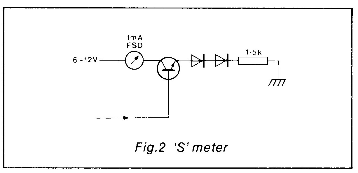
The AGC output from IC5 is applied to the two IF stages via 100 ohm resistors (R7 & R8) and is also taken off the board to act as S-Meter drive. The AGC line has a value of about 2V at the AGC threshold and it increases by about 12.5 mV for each dB increase in signal (80 dB/V). The 2V threshold is temperature-dependent and may be compensated by silicon diodes. A simple S-Meter which is generally adequate is shown in Fig. 2. The 1.5 kohm resistor may need some slight adjustment to give the correct range.
The capacitor C21 shown in the circuit diagram should not be necessary if the receiver is to be used for speech only and will probably not be necessary with CW. However, under some circumstances, it is possible to find low frequency instability in the AGC system during the reception of CW. The insertion of C21, which may have a value between 0.1 and 1.0 µF, cures it.
The audio output stage uses an SL6310, an audio power amplifier in an 8-lead minidip package capable of delivering between 800 mW and 1 W with a 12V supply. If more than 800 mW of audio is needed the SL6310 should be omitted from the board and an external high power amplifier used. The SL6310 requires a loudspeaker of 8 ohms or more.
THE TRANSMITTER
This section is more accurately described as the sideband exciter. It uses two integrated circuits (IC8 and IC9) and a transistor (TR4). IC9 is an audio amplifier with AGC which is used to ensure that the output of the transmitter is substantially unchanged by varying audio input levels. Such a circuit is known as a VOGAD (Voice Operated Gain Adjusting Device).
These circuits require the use of a low impedance microphone (500 ohms or less) with an output in the range 1-30 mV. The AGC range is about 60 dB, which may be too large for some applications where high levels of background noise are present; it may be reduced by connecting a 1 kohm resistor R32 in parallel with C47. If this resistor is used C47 should be increased from 4.7 nF to 47 nF to preserve the HF rolloff characteristic of the VOGAD.
The two capacitors C52 and C53 isolate the VOGAD inputs at DC and the capacitors C50 and C51 decouple any RF which may be induced on the microphone leads. The audio from the VOGAD is coupled to the double-balanced modulator IC8 by C46.
As in the receiver IC8 may be either an SL1640 or an SL1641, and again a 330 ohm resistor R28 is required only if the SL1641 is used.
The principle of single sideband generation used in this transmitter is simple. Audio and carrier are applied to the double-balanced modulator, the output of which consists of a DSBSC (double sideband suppressed carrier) signal which is filtered in a narrow filter to remove one sideband. Which sideband is selected depends on the carrier frequency chosen.
The DSB signal from IC8 is amplified and buffered by TR4 and applied to the crystal filter. TR4 is a high frequency PNP transistor; in this design a 2N5771 is specified but any high frequency silicon PNP transistor with a low Cob would be suitable. A transistor is used in this buffer rather than an integrated circuit because it does not present any load to the filter when it is turned off during reception. The gain of TR4 amplifier is set by R26 and may be altered if necessary. Bias for TR4 is obtained by direct coupling from the double-balanced modulator.
THE SIDEBAND OSCILLATORS
Each oscillator uses a Siliconix J304 FET (TR2 and TR3) in a Colpitts circuit. The quartz crystals supplied with the XF9-B or OC1246AX filters are 30 pF parallel resonant types and the oscillators are designed to work with these. If 20 pF parallel resonant types are used it is probably sufficient to reduce C32, C33, C34 and C35 to 33 pF each but if series resonant crystals are to be used more changes will be necessary. The trimmer capacitors C31 and C38 are used for fine adjustment of the USB (8.9985 MHz) and LSB (9.0015 MHz) crystals respectively.
The output voltage from both oscillators is developed across R24. In the prototypes R24 is 68 ohms and the output voltage is about 80 mV rms. If this voltage falls outside the range 60-200mV rms
2 then R24 should be adjusted until the voltage is within this range.
The oscillator to be used is selected by switching the 12V supply to its power input pin. The other oscillator's power supply should be off and, preferably, grounded.
CONSTRUCTION
The printed circuit board layout for this transceiver is shown in Fig. 3 (a) and the component placing in Fig. 3 (b). The drilling detail is shown in Fig. 3 (c), and the components used are listed below.


The resistors are metal film 0.25 W types. Capacitors below 1 nF are miniature ceramic types. Capacitors between 1 nF and 100 nF are miniature monolithic ceramic types with 2.5 mm (0.1 in) lead spacing, and all capacitors above 100 nF with the exception of C6 (an aluminium electrolytic) are miniature resin dipped tantalum electrolytics. The transformers T1 and T2 are wound on blocks of B1 ferrite 11.3 x 11.3 x 5.8 mm (0.5 in x 0.5 in x 0.25 in) with two holes. These blocks are fixed to the circuit board with epoxy resin and then wound with 32-36 SWG self-fluxing copper wire. T1 has a two-turn primary (on the D1 side) and a six turn secondary; T2 has six turns on each.
There are four wire links on the board to connect various earth tracks together for minimum HF impedance. Through a hole near the quartz crystals passes a piece of wire which is soldered (as quickly as possible to avoid damage) to the crystal cans to ground them.
All components must be mounted with the shortest possible leads and integrated circuit sockets must not be used.
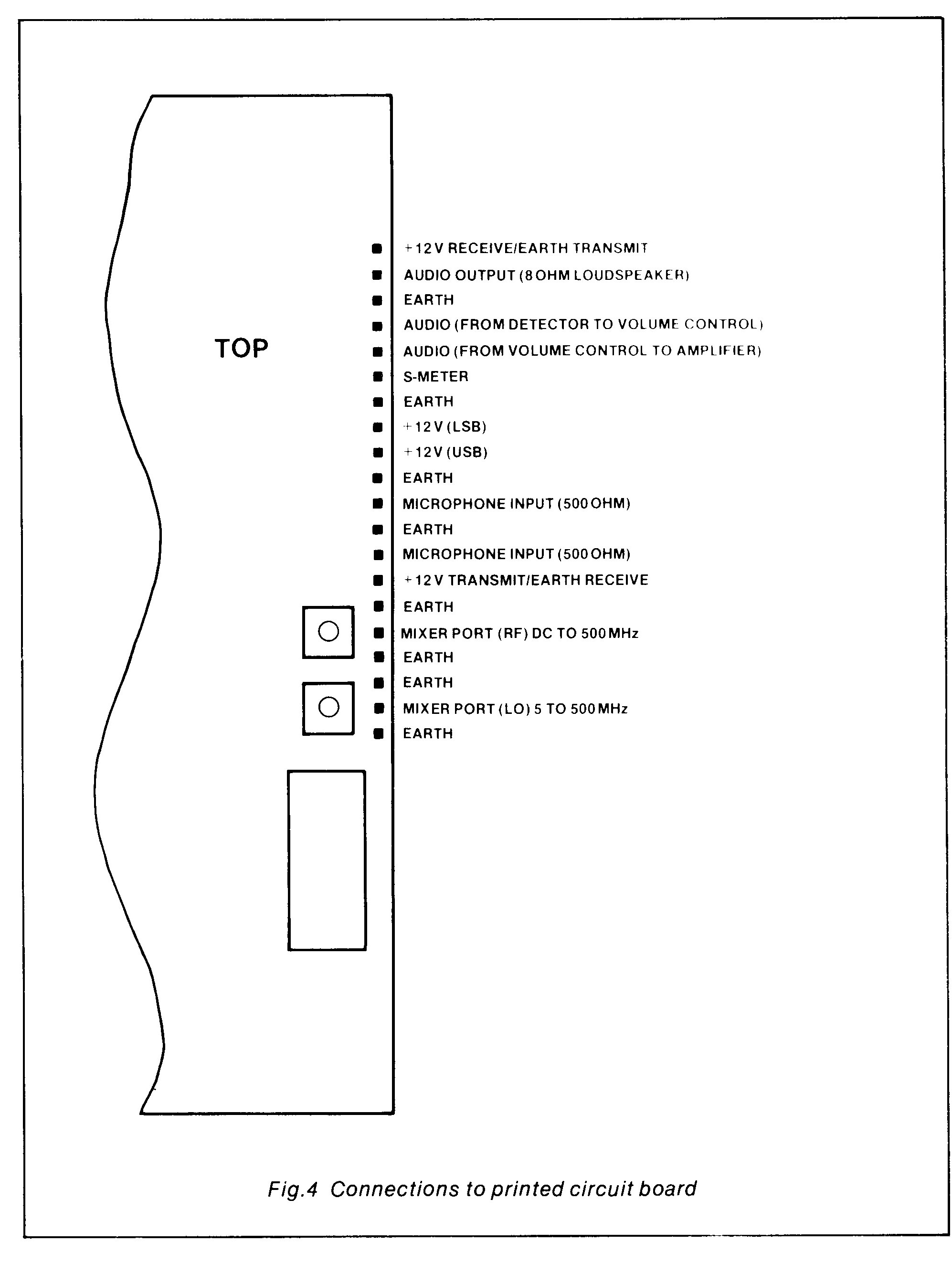
The connections to the board are illustrated in Fig. 4. The RF and local oscillator signals may either be connected via the same 2.5 mm (0.1 in) pitch connections as the rest of the signals and supplies or via miniature SMA or SMB co-axial sockets.
The board is powered from a single +12V supply. It will, however, operate satisfactorily between +10V and +15V without damage or significant change in performance. It is essential to ground the transmitter supply during reception and the receiver supply during transmission. This is not merely to prevent spurious transmission of signals but because these other lines are actually used as DC return paths.
When the board is complete the sideband oscillators should be set up by connecting a frequency meter across R24 and connecting power to each oscillator and adjusting its trimmer until its frequency is within 10 Hz of nominal.
 CONNECTION AND USE
The use of the board is illustrated in Fig. 5. In addition to this board all that is required is a local oscillator capable of delivering 500 mV rms into 50 ohms, a preselector (with a pre-amplifier at VHF if a small antenna is to be used), an RF power amplifier, a 12V 200 mA power supply, and a microphone, volume control and loudspeaker. An S-Meter circuit as described above is an optional extra.

The circuit board is checked out in a similar circuit to that shown except that test equipment replaces some or all of the blocks external to the board. If for any reason the board does not perform properly when first connected it should be checked for short-circuits and then the integrated circuits should be checked with a high impedance voltmeter for correct operating voltages. If this method also fails then signals must be traced through the board with the aid of a signal generator and an oscilloscope or spectrum analyser.
Footnotes
1 The MD-108 has an elder (and more expensive) brother called the MD 138 which has a higher third-order intercept point but there is no point in using it in this particular design since the intermodulation performance of the system is set by the mixer, the bi-directional amplifier and the filter and improving one without improving the others will do little for the overall performance of the system.
2 This is not very likely to happen since the prototype boards all had outputs lying between 70 and 100 mV and they used FETs from a number of batches and crystals of widely varying activity.
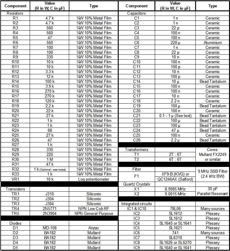
TABLE 1 - Component List